- 您现在的位置:买卖IC网 > Sheet目录1993 > DS1123LE-100+ (Maxim Integrated Products)IC DELAY LINE 256TAP 16-TSSOP
DS1123L
3.3V, 8-Bit, Programmable Timing Element
____________________________________________________________________
13
Application Information
Power-Supply Decoupling
To achieve the best results when using the DS1123L,
decouple the power supply with a 0.01F and a 0.1F
capacitor. Use high-quality, ceramic, surface-mount
capacitors, and mount the capacitors as close as possi-
ble to the VCC and GND pins of the DS1123L to mini-
mize lead inductance. The DS1123L may not perform as
specified if good decoupling practices are not followed.
Unused Inputs When Using the Serial-
Programming Mode
When using the serial-programming mode, the unused
parallel inputs must be connected to VCC or GND to pre-
vent them from floating and drawing excessive current.
Test Conditions
INPUT:
Ambient Temperature:
25°C ± 3°C
Supply Voltage (VCC):
3.3V ± 0.1V
Input Pulse:
High = 3.0V ± 0.1V
Low = 0.0V ± 0.1V
Source Impedance:
50
Ω (Max)
Rise and Fall Times:
3.0ns (Max) (Measured
Between 0.6V and 2.4V)
Pulse Width:
500ns
Period:
1s
OUTPUT: The outputs are loaded with a 74F04. Delay
is measured between the 1.5V level of the rising or
falling edge of the input signal and the corresponding
edge of the output signal.
NOTE: Above conditions are for test only and do not
restrict the operation of the device under other data
sheet conditions.
PART
STEP SIZE
(ns)
MAX DELAY TIME AND
MAX PULSE WIDTH*
(ns)
MAX INTEGRAL
NONLINEARITY
(ns)
MAX INPUT
FREQUENCY
(MHz)
MIN INPUT PULSE
WIDTH
(ns)
DS1123L-25
0.25
63.75
±2
25
40
DS1123L-50
0.5
127.5
±2
25
40
DS1123L-100
1.0
255
±4
25
40
DS1123L-200
2.0
510
±5
25
40
Table 1. DS1123L Delay Line/PWM Ranges and Tolerances
*
This is the maximum delay in normal mode (MS = 0) measured with respect to the reference output, and the maximum pulse width
in monostable vibrator mode (MS = 1).
PART
PERIOD CHANGE/STEP
(ns)
MIN OSCILLATOR FREQUENCY
(MHz)
MAX OSCILLATOR FREQUENCY*
(MHz)
DS1123L-25
0.5
6.6
22
DS1123L-50
1.0
3.6
22
DS1123L-100
2.0
1.9
22
DS1123L-200
4.0
0.98
22
Table 2. DS1123L Adjustable Oscillator Characteristics
*
Maximum output frequency depends on the actual step-zero delay value. Worst-case values are shown in the table. Output period
is equal to 2 x tD, where tD = delay value referenced to IN.
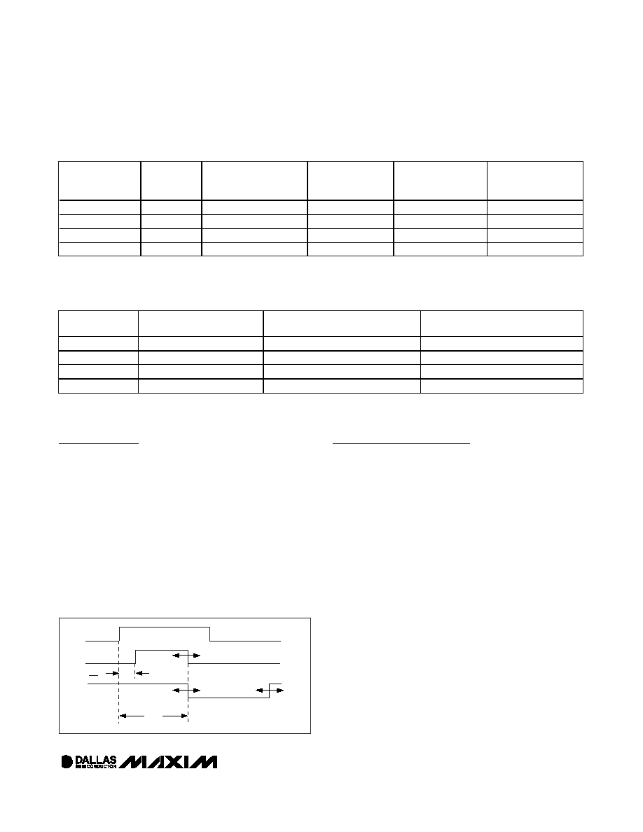
IN
PWM
OUT
tREF
tD
Figure 10. Output Timing Diagram for MS = 1
发布紧急采购,3分钟左右您将得到回复。
相关PDF资料
DS1124U-25+T
IC DELAY LINE 256TAP 10-USOP
DS1135LU-300/T&R
IC DELAY LINE 300NS 8-USOP
DS1135Z-12/T&R
IC DELAY LINE 12NS 8-SOIC
DS1181LE+
IC CLOCK MOD SS 8-TSSOP
DS1243Y-120
IC NVSRAM 64KBIT 120NS 28DIP
DS1244W-120IND
IC NVSRAM 256KBIT 120NS 28DIP
DS1248Y-70IND
IC NVSRAM 1MBIT 70NS 32DIP
DS1251WP-120+C02
IC NVSRAM 34PWRCP
相关代理商/技术参数
DS1123LE-200
功能描述:延迟线/计时元素 Programmable 3.3V 8 Bit Timing Element RoHS:否 制造商:Micrel 功能:Active Programmable Delay Line 传播延迟时间:1000 ps 工作温度范围: 封装 / 箱体:QFN-24 封装:Tube
DS1123LE-200+
功能描述:延迟线/计时元素 Programmable 3.3V 8 Bit Timing Element RoHS:否 制造商:Micrel 功能:Active Programmable Delay Line 传播延迟时间:1000 ps 工作温度范围: 封装 / 箱体:QFN-24 封装:Tube
DS1123LE-25
功能描述:延迟线/计时元素 Programmable 3.3V 8 Bit Timing Element RoHS:否 制造商:Micrel 功能:Active Programmable Delay Line 传播延迟时间:1000 ps 工作温度范围: 封装 / 箱体:QFN-24 封装:Tube
DS1123LE-25+
功能描述:延迟线/计时元素 Programmable 3.3V 8 Bit Timing Element RoHS:否 制造商:Micrel 功能:Active Programmable Delay Line 传播延迟时间:1000 ps 工作温度范围: 封装 / 箱体:QFN-24 封装:Tube
DS1123LE-50
功能描述:延迟线/计时元素 Programmable 3.3V 8 Bit Timing Element RoHS:否 制造商:Micrel 功能:Active Programmable Delay Line 传播延迟时间:1000 ps 工作温度范围: 封装 / 箱体:QFN-24 封装:Tube
DS1123LE-50+
功能描述:延迟线/计时元素 Programmable 3.3V 8 Bit Timing Element RoHS:否 制造商:Micrel 功能:Active Programmable Delay Line 传播延迟时间:1000 ps 工作温度范围: 封装 / 箱体:QFN-24 封装:Tube
DS1123LS-200
功能描述:延迟线/计时元素
RoHS:否 制造商:Micrel 功能:Active Programmable Delay Line 传播延迟时间:1000 ps 工作温度范围: 封装 / 箱体:QFN-24 封装:Tube
DS1123LS-25
功能描述:延迟线/计时元素
RoHS:否 制造商:Micrel 功能:Active Programmable Delay Line 传播延迟时间:1000 ps 工作温度范围: 封装 / 箱体:QFN-24 封装:Tube